Summary:A research team from the University of Delaware has developed cutting-edge technology for photonics devices that could enable faster communications between phones and computers.
If you use a smartphone, laptop, or tablet, then you benefit from research in photonics, the study of light. At the University of Delaware, a team led by Tingyi Gu, an assistant professor of electrical and computer engineering, is developing cutting-edge technology for photonics devices that could enable faster communications between devices and thus, the people who use them.
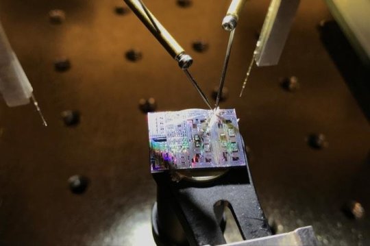
The research group recently engineered a silicon-graphene device that can transmit radiofrequency waves in less than a picosecond at a sub-terahertz bandwidth — that’s a lot of information, fast. Their work is described in a new paper published in the journal ACS Applied Electronic Materials.
“In this work, we explored the bandwidth limitation of the graphene-integrated silicon photonics for future optoelectronic applications,” said graduate student Dun Mao, the first author of the paper.
Silicon is a naturally occurring, plentiful material commonly used as a semiconductor in electronic devices. However, researchers have exhausted the potential of devices with semiconductors made of silicon only. These devices are limited by silicon’s carrier mobility, the speed at which a charge moves through the material, and indirect bandgap, which limits its ability to release and absorb light.
Now, Gu’s team is combining silicon with a material with more favorable properties, the 2D material graphene. 2D materials get their name because they are just a single layer of atoms. Compared to silicon, graphene has better carrier mobility and direct bandgap and allows for faster electron transmission and better electrical and optical properties. By combining silicon with graphene, scientists may be able to continue utilize technologies that are already used with silicon devices — they would just work faster with the silicon-graphene combination.
“Looking at the materials properties, can we do more than what we’re working with? That’s what we want to figure out,” said doctoral student Thomas Kananen.
To combine silicon with graphene, the team used a method they developed and described in a paper published in 2018 in npj 2D Materials and Application. The team placed the graphene in a special place known as the p-i-n junction, an interface between the materials. By placing the graphene at the p-i-n junction, the team optimized the structure in a way that improves the responsivity and speed of the device.
This method is robust and could be easily applied by other researchers. This process takes place on a 12-inch wafer of thin material and utilizes components that are smaller than a millimeter each. Some components were made at a commercial foundry. Other work took place in UD’s Nanofabrication Facility, of which Matt Doty, associate professor of materials science and engineering, is the director.
“The UD Nanofabrication Facility (UDNF) is a staff-supported facility that enables users to fabricate devices on length scales as small as 7 nm, which is approximately 10,000 times smaller than the diameter of a human hair,” said Doty. “The UDNF, which opened in 2016, has enabled new research directions in fields ranging from optoelectronics to biomedicine to plant science.”
The combination of silicon and graphene can be used as a photodetector, which senses light and produces current, with more bandwidth and a lower response time than current offerings. All this research could add up to cheaper, faster wireless devices in the future. “It can make the network stronger, better and cheaper,” said postdoctoral associate and the first author of the npj 2D Materials and Application article Tiantian Li. “That is a key point of photonics.”
Now the team is thinking about ways to expand the applications of this material. “We’re looking at more components based on a similar structure,” said Gu.
This work is funded by grants from AFOSR and NASA, and the team has a partial collaboration with Bell Labs.
More:Science Daily


Leave a Reply
You must be logged in to post a comment.